|
|
 |
 |
 |
RESEARCH & PROJECTS
|
The
mission of the Inter-University Consortium for Nanoelectronics
(referred to as IUNET) is that of fostering collaboration of Italian
University teams active in the fields of Semiconductor Science and
Technology, device Physics and Nanoelectronics, with Research
Institutes and Industry. This goal is pursued by promoting
participation to European Projects, where IUNET acts as a unified
interface to the project partners, selects the participating
Universities, and nominates an internal coordinator.
The research
activity addresses three macro-areas referred to as:
More
Moore

|
This
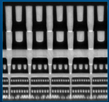
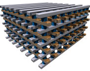
activity addresses the leading edge of the CMOS Semiconductor
Technology for both logic and memory applications. New device
structures are proposed for improved short-channel effects, power
consumption, performance and reliability. Also, novel memory concepts
like phase-change cells (PCM) are likely to play a major role in future
computer architecture.
|
More than Moore

|
Several
semiconductor applications do not require a leading-edge technology for
logic but, rather, special devices able to sustain high voltages and to
deliver high power to an external load; solar cells for generation of
renewable energy, and FETs able to operate at microwave frequencies for
the analog treatment of communication signals.
|
- Microwave and Hyperfrequencies semiconductor devices (MESFET,
HEMT, HBT)
-
Power and smart-power devices
-
High-efficiency solar cells, smart grids and energy harvesting
tools
-
Sensors, biosensors and sensor networks
- Large area electron devices on low-cost organic substrates, or
glass (Displays, solar cells, sensors, etc)
Beyond CMOS

|
This
area investigates disruptive technologies based on alternative device
concepts, like magnetic, ferroelectric or resistive memory and logic
devices, or entirely-new materials like organic semiconductors,
graphene and, more generally, two-dimensional materials for large-area
Electronics. Also, graphene nanotubes exhibit interesting properties as
miniaturized FETs.
|
- Novel electron devices based on two-dimensional materials
(Graphene, MoS, etc)
- Alternative memories (Memristors, STTM, etc)
PROJECTS
FP7
Projects
ENIAC
Projects
H2020
Pojects
ECSEL
projects
HORIZON EUROPE Projects
FLAG-ERA
Project
PON Projects
|
 |
|


